
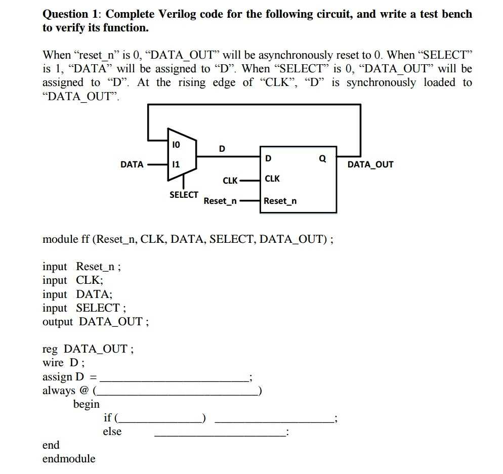
Sequence detection is a fundamental function in digital design and is often used in various applications, such as data communication, error correction, and pattern recognition. A sequence detector is a combinational circuit that detects a specific sequence of input signals and generates an output signal when the sequence is detected.
In this article, we will discuss how to write a sequence detector Verilog code with a test bench. Verilog is a hardware description language (HDL) that is widely used in the digital design industry for designing and verifying electronic systems. It allows designers to describe the behavior of a digital system at different levels of abstraction, such as behavioral, dataflow, and structural.
The Verilog code for a sequence detector typically consists of two parts: the design module and the test bench module. The design module describes the functionality of the sequence detector circuit, while the test bench module provides stimulus to the design module and verifies its outputs. The test bench module is responsible for generating input stimuli, applying them to the design module, and checking the correctness of the output signals.
Writing a sequence detector Verilog code with a test bench involves defining the input and output signals, specifying the sequential logic to detect the desired sequence, and writing test cases to verify the correctness of the design. By simulating the Verilog code using a simulation tool, such as ModelSim or Xilinx Vivado, designers can observe the behavior of the sequence detector and ensure its functionality.
What is a sequence detector?

A sequence detector is a digital circuit that is designed to detect a specific pattern or sequence of input signals. It is commonly used in various applications, such as communication systems, data processing, and control systems. The sequence detector operates by analyzing the input signals and generating an output signal when the desired sequence is detected.
The input signals can be binary digits (0 or 1) or any other type of digital signals. The desired sequence can be a simple pattern with only a few bits or a more complex pattern with multiple bits. The sequence detector circuit typically consists of combinational logic elements, such as gates and flip-flops, which are interconnected to perform the desired sequence detection.
There are different types of sequence detectors, depending on the specific requirements and characteristics of the desired sequence. Some common types include simple sequence detectors that detect a specific bit pattern, overlapping sequence detectors that detect a pattern that can overlap with itself, and finite state machines that can detect complex sequences with multiple states and transitions.
Sequence detectors are an essential component in many digital systems and play a crucial role in ensuring the correct operation and processing of input signals. They are often used in error detection and correction, data compression and decompression, and various other applications where the detection of specific patterns is necessary.
Overview of Verilog Code
Verilog code is a hardware description language used for designing and simulating digital circuits. It allows engineers to model and test complex systems before implementation in hardware. The Verilog code consists of modules, which are building blocks for creating larger and more complex circuits. Each module can be instantiated and interconnected to form a complete digital system.
At a high level, a Verilog code is divided into two main sections: the module declaration and the module body. The module declaration defines the input and output ports of the module, while the module body contains the actual implementation of the circuit. The Verilog code uses a combination of procedural and concurrent statements to describe the behavior and structure of the circuit.
The test bench is an essential part of Verilog code as it allows engineers to verify the functionality of the circuit. It generates input stimulus and checks the output response against the expected results. By simulating the Verilog code with the test bench, engineers can identify and fix any design issues before proceeding to the physical implementation.
In the case of a sequence detector, the Verilog code will include the logic for detecting a specific sequence of inputs. This can be achieved using combinational or sequential logic circuits, such as state machines or shift registers. The test bench will provide a set of input sequences to verify the correctness of the sequence detection circuit.
Overall, Verilog code is a powerful tool for designing and simulating digital circuits. It allows engineers to describe, test, and refine complex systems before committing to physical implementation. By using Verilog, engineers can save time and resources by identifying and fixing design issues early in the development process.
Designing the sequence detector
When designing a sequence detector in Verilog, there are several key steps to consider. First, you need to define the sequence that you want to detect. This can be done by identifying the specific pattern or sequence of inputs that you are interested in recognizing. For example, you may want to detect a specific series of bits or a certain combination of signals.
Once you have defined the sequence, the next step is to create a state diagram that outlines the different states and transitions that the detector will go through. Each state represents a specific condition or combination of inputs, and the transitions indicate how the detector moves between states based on the input it receives. This state diagram serves as a blueprint for the implementation of the sequence detector.
In Verilog, the sequence detector can be implemented using finite state machines (FSMs). Each state in the state diagram can be represented by a separate module or a set of combinational and sequential logic elements. The inputs to the module would correspond to the signals that the detector receives, and the outputs would indicate when the desired sequence has been detected.
Once the Verilog code for the sequence detector is written, it is important to verify its functionality by creating a test bench. The test bench provides a way to simulate different input scenarios and check if the detector correctly detects the desired sequence. This involves creating a set of test cases with different input patterns and verifying that the outputs match the expected results.
Overall, designing a sequence detector requires careful planning and attention to detail. By defining the sequence, creating a state diagram, implementing the Verilog code, and testing the functionality, you can ensure that the detector accurately recognizes the desired pattern or sequence of inputs.
Writing the verilog code

When writing the verilog code for a sequence detector, there are several steps that need to be followed. First, the input and output ports of the module need to be defined. In this case, the input will be a clock signal and a reset signal, while the output will be a sequence detection signal. These ports can be declared using the ‘input’ and ‘output’ keywords.
Next, the internal variables and registers need to be defined. In this case, a shift register will be used to store the incoming bits and check for the desired sequence. The size of the shift register will depend on the length of the sequence being detected. The syntax for declaring a register is ‘reg [size-1:0] register_name;’
After declaring the ports and registers, the logic for the sequence detection needs to be implemented. This can be done using a combination of if-else statements and logical operators. In each clock cycle, the incoming bit is shifted into the shift register. Then, the contents of the register are compared to the desired sequence using if-else statements. If the sequence is detected, the output signal is set high.
Finally, a test bench needs to be written to simulate the behavior of the sequence detector module. The test bench will generate a clock signal and provide input values to the module. It will also monitor the output signals and compare them to the expected values. The test bench can be written using the same verilog syntax as the module, but with additional code for generating the clock signal and monitoring the signals.
In conclusion, writing the verilog code for a sequence detector involves defining the input and output ports, declaring internal variables and registers, implementing the sequence detection logic, and writing a test bench to verify the functionality of the module. Following these steps will help ensure that the sequence detector performs as expected.
Creating a test bench
In digital design, a test bench is a piece of code that is used to verify the functionality of a design. It provides a set of test inputs and checks if the outputs of the design match the expected results. In the context of a sequence detector verilog code, a test bench would be used to test the functionality of the sequence detector design.
When creating a test bench for a sequence detector, several key steps need to be followed. First, the desired test sequence needs to be defined. This sequence will be used as the input to the sequence detector under test. The test bench then needs to generate the clock and reset signals required for the design. These signals help simulate the operation of the design in a controlled manner.
The test bench should also include a monitor module to capture the output of the sequence detector. This module compares the actual output of the design with the expected output and generates an assertion error if there is a mismatch. Additionally, the test bench can include stimulus generation code to automate the test sequence generation process. This ensures that multiple test cases can be executed efficiently.
Furthermore, it is important to include code in the test bench that facilitates the checking and reporting of test results. This can be done using specific Verilog assertions or by monitoring specific signals and generating appropriate output messages. Finally, the test bench should be run using a Verilog simulator to execute the test cases and verify the correctness of the sequence detector design.
Testing and Debugging the Sequence Detector
Testing and debugging are crucial steps in the development process of any digital design, including a sequence detector. In this section, we will discuss the various approaches and techniques to effectively test and debug a sequence detector implementation in Verilog.
1. Test Bench Development
The first step in testing a sequence detector is to develop a test bench. A test bench is a Verilog code that stimulates the inputs of the sequence detector and captures the outputs for verification. It is essential to create a comprehensive test bench that covers all possible scenarios and edge cases.
The test bench should include test cases for both valid and invalid input sequences. It should also incorporate different timing scenarios, such as varying input signal durations and delays. By covering a wide range of test cases, we can ensure the robustness and correctness of the sequence detector implementation.
2. Test Case Execution and Verification
After developing the test bench, it is time to execute the test cases and verify the results. During the test case execution, the test bench will stimulate the inputs of the sequence detector and capture its outputs.
The captured outputs should be compared against the expected outputs for each test case. Any discrepancies or errors indicate a potential bug or issue in the sequence detector implementation. It is crucial to carefully analyze and debug any failures to identify and fix the underlying problems. This may involve examining the waveform and signal traces to pinpoint the problematic areas in the design.
3. Debugging Techniques
Debugging a sequence detector can be a challenging task. Here are some effective techniques for debugging:
- Signal Tracing: Use waveform viewers to trace the values and timing of different signals in the design. This can help identify incorrect signal transitions or unexpected behavior.
- Assertion-Based Verification: Incorporate assertions into the test bench to automatically check for expected conditions during simulation. Assertions can help catch design flaws or violations of desired properties.
- Incremental Testing: Divide the testing process into smaller steps and test each component or sub-module separately before integrating them into the complete sequence detector. This approach allows for easier isolation and debugging of potential issues.
- Debugging Statements: Insert debug print statements in the Verilog code to monitor the internal state or variables of the sequence detector. This can provide insights into the execution flow and help identify problematic areas.
Summary
In conclusion, testing and debugging are crucial steps in the development of a sequence detector. By developing a comprehensive test bench, executing test cases, verifying the results, and using effective debugging techniques, we can ensure the correctness and reliability of the sequence detector implementation.